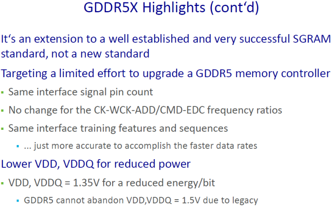
The final specification for GDDR5X (successor to GDDR5) has been decided and the gap is trimmed a bit between HBM and HBM2 in terms of performance. Well, implementing GDDR5X is easier than other upcoming alternatives, requiring just a few tweaks in the GPU design. The new technology is designed to improve bandwidth to get high-performance graphics processing units without fundamentally changing the memory architecture of graphics cards or memory technology itself. 
The new 16n prefetch architecture, which enables up to 512 bit (64 Bytes) per array read or writes access, is one of the key improvement of the GDDR5X standard compared to the predecessor. The older GDDR5 featured 8n prefetch architecture and could read or write up to 256 bit (32 Bytes) of data per cycle. One thing common between both GDDR5 and GDDR5X is their use of two different clock types. A differential command clock (CK) to where address and command inputs are referenced, as well as a forwarded differential write clock (WCK) where read and write data are referenced. WCK runs at a frequency that is two times higher than the CK. The data can be transmitted at double data rate (DDR) or quad data rate (QDR) relative to the differential write clock (WCK), depending whether 8n prefetch or 16n prefetch architecture and protocols are used. Accordingly, if makers of chips manage to increase CK clock to 1.5 GHz, then data rate in QDR/16n mode will rise to 12 Gbps.
As for the data rates, JEDEC’s GDDR5X SGRAM announcement points at a range of 10 to 14 Gbps but Micron believes that the actual limit will touch 16 Gbps mark in the future. It’s hard to believe because a commercial chip running such high rates has been never seen before. However, even a 256-bit GDDR5X memory sub-systems running at 14 Gbps could provide up to 448 Gbps of memory bandwidth, just 12.5% lower compared to that of AMD’s Radeon R9 Fury X (which uses first-gen HBM).
Currently, Micron is able to ship two different densities, 8Gb and 16Gb that can allow for VRAM of up to 16GB over a 256-bit wide memory bus. As for the energy efficiency, Micron has implemented a number of ways to keep power consumption of the new graphics DRAM in check. GDDR5X’s supply voltage and I/O voltages are decreased from 1.5V to 1.35V. To cut power consumption of the new memory by up to 10%, Vdd and Vddq were reduced. It is important for high-performance and mobile devices where the memory can take a noticeable chunk of the available power budget.
The internals of GDDR5X is completely different from the current GDDR5X. The transition of the industry to GDDR5X is just a small step as HBM DRAM is on the way. Implementation of GDDR5X should not be too expensive both from R&D and production perspectives; at least, this is something that Micron implied several months ago when it revealed the first details about the technology.


