So, all of us know a computer. If you are looking at this, it’s highly likely that you are looking at it from a PC or a smartphone. But have we ever wondered how we get the hearts and brains of these devices? Irrespective of whether one is a veteran making PC’s since 1989 or amateur to the trade of PC building, looking for advice to his new PC, there is one thing that DIY builders will always appreciate more. And that is “information.” In this post, we try to discuss a very specified topic of that information, and that is process technology.
If you have wandered even a bit into technology forums, like Anandtech, Tomshardware or Semiaccurate, you must have come across terms like 14nm, 22nm, finfets, “real 14nm”, node ( or rarer topics like FDSOI, PDSOI, FDX ) etcetera. So what IS this process technology, why are these even relevant, and why can knowing a bit more about these help you in the long run?
WHO MAKES CHIPS?

Before we get into the nitty-gritty of the technical analysis, let us first look into the basics. A computer chip is primarily made from silicon. And the place where it is made is typically called a fab or a fabrication plant. Production of a fabrication plant is a very costly affair. Thus we can only find a handful of companies with very high capital that can actually even afford to create a fabrication plant. As of 2016, there are very few major players in the fab industry. Listed in no particular order, are:

1. TSMC (Taiwanese Semiconductor Manufacturer Comp.): – Based in Taiwan, but owning plants at a variety of places, TSMC is one of the highest volume chipmakers in existence right now. Commanding the supplies of major corporations like Apple and Nvidia, as well as smaller companies like MediaTek and Rockchip, they are a major force to reckon with. Their most celebrated offering is the TSMC 16nm node, which comes in 3 flavors, including 16FF, 16FF+ and 16FFC where FF stands for FinFet and C stands for compact. TSMC has plans to sample even smaller nodes like 10nm and 7nm as early as 2017.

2. Samsung Fabs: – Based in South Korea, this omnipresent brand makes chips for a variety of companies, like Qualcomm and Nvidia. Coming in at a close second to TSMC, Samsung offers a variety of nodes, and commands high volume, undercutting a TSMC supply chain strangled by Apple’s high volume demands. Currently, their most celebrated node is the 14nm node, which again, comes in 3 flavors—14LPP, 14LPE, and 14LPC—with plans ongoing for a 14LPH. LP stands for Low Power, P and E stands for Plus and Early respectively. H stands for High Performace.

3. Global Foundries: – Currently owned by the Government of Abu Dhabi as a subsidiary of Mubadala corp. The AMD spinoff; Global Foundries, or Glo Flo has just recently come over a bad patch of time with one of their own nodes ( 14nm XM ) being canned for the 14LPP and 14LPE being licensed from Samsung. However after IBM sold off their process division to Glo Flo, it seems to be on track for recovering itself under the very apt leadership of Sanjay Jha ( ex-Motorola CEO ). Currently the owner of the “only true” High-Performance 14nm node ( inherited from IBM ), Glo Flo seems to be on track for delivering their 7nm process by 2019. They also offer a 22nm FDSOI called 22 FDX and have plans for a 12nm FDSOI offering as 12FDX. Their primary customers for the 14nm node include AMD and Cavium, with AMD using it for their hotly anticipated “Summit Ridge (ZEN/Ryzen)” cpus as well as their Polaris GPU’s.

4. Intel:- Arguably the owners of the best Fab on this planet, Intel is noted not only for its high performance and low-density nodes, but also for the tremendous amount of investment it does in research and development of a new Fab. Currently, Intel offers 14nm node as their best node in their famed Broadwell, Skylake and Kabylake processors. Also, they were the ones that pioneered the use of FinFets in their flawless 22nm node. However, they are facing some rough patches as of recently. With their own 14nm node facing multiple delays and their proposed 10nm delayed.
Apart from these four major competitors, there are also others who offer a Fab.
1. STMicro A: – An old player in the market, though unfortunately never enjoyed the significance others did. They have a 28nm FDSOI node.
2. UMC: – A united conglomerate of companies from Taiwan. It had plans for a FinFet tapeout in late 2015.
INSIDE THE SANDS OF TIME:-

The process of making chips is a fascinating process, but unfortunately, it contains multiple technical jargons. But as a preliminary, let us try to understand the very basic idea behind a typical fab procedure
The first stage for any chip manufacturing is the “blueprint” of the chip, which is known by the name, the”Circuit Diagram”. Making one is a Herculean task by itself, and requires several man hours from brilliant minds all over the company. The circuit diagram is then printed in what can be called to be the layout of the chip—or the “Mask”. When the mask is complete, it is sent to the Fabs for manufacturing chips.

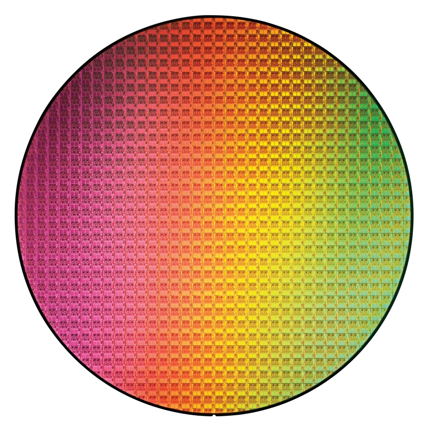
The Fabs are a huge area which is aggressively made dust free. Dust is impurities that can meld easily inside silicon to produce defects in the chips. An operation theatre contains over 100-1000 times the amount of dust in a typical fab. At the Fabs, first a lot of sand is taken. Sand contains quartz, a crystalline form of silicon. And a huge monolithic crystal mound is made from this quartz, making a silicon lattice perfectly aligned. This alignment is critical, as misalignment could mean leakage, and dysfunction of that portion of the silicon die. This procedure is achieved by rotating molten silicon around a central zone. The silica crystallises around  itself, giving it the familiar circular disc, or a “wafer”. This silicon wafer is then sent to the next processing stage.
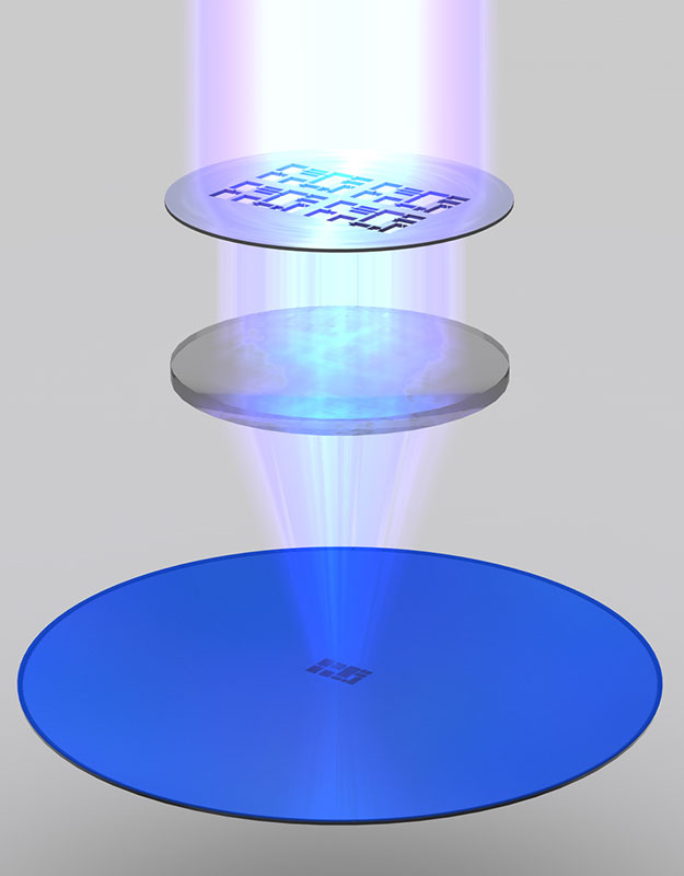
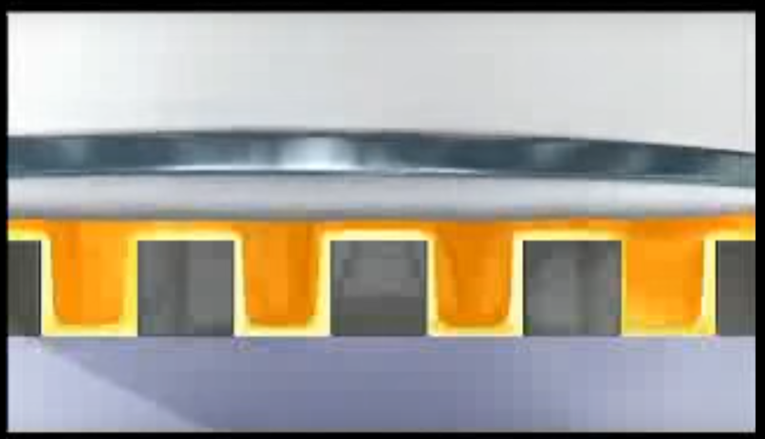
A wafer is then coated with a photosensitive resistive coating via spin coating, and light is used directly on it, through the mask. The ultraviolet rays react with the photosensitive material to leave the imprint of the mask. The wafer is then washed away to remove the reacted coating, creating a very spiked structure somewhat similar to this. This wafer is then coated with an insulator material, to arrest electric leakage. This indention or the valley design are what creates the switches—the transistors.

The next stage in this complicated process is the establishment of the conductivity of silicon. This is established by an old procedure called doping. Doping involves implanting doped atoms into the silicon lattice so that the silica is replaced by more conductive dope atoms. After a wafer is doped, copper is then electro-etched into wafer and the wafer is sufficiently smoothed so that no 2 copper fillings in the trenches can touch each other. Thus the wafer die is completely ready to be cut into pieces. The whole process takes in the neighborhood of 2 months from start to completion.
Thus, after a hefty process, we finally have a working piece of silicon, made by a Planar lithographic process. In the next posts, we discuss the FinFETs and SOI’s.


