Ryzen : A Small history behind the phenomenon
After 5 years , of waiting we finally have the AMD Ryzen processors featuring the AMD “Zen” core. It brings AMD back to the competitive paradigm. In this article, we try to explore in depth at least some parts of the execution engines that went inside the successful product.
The development of Zen started in 2012 when Jim Keller was rehired from Apple. Jim is a chip veteran, with successful and revolutionary processors under his name, like the AMD K-7 and the Apple A5 Typhoon. Finally, the processor was released as a successful product in the first quarter of 2017. Other than Jim, the team also consisted of Mike Clark, Suzanne Plummer, Teja Singh, Lyndal Curry, Mike Tuuk, Farhaan Rahman, Andy Halliday, Matt Crumm, Mike Bates, and Joshua Bell. Armed with their hard work AMD promised us a 40% improvement in the IPC (average) compared to their previous generation.

A Dive into the Architecture
Zen in essentially a new design, making a departure from AMD’s previous shared FPU approach that it used in its Bulldozer family of processors. Rather than the clustered design Zen uses a traditional layout of 4 cores in a tightly integrated package, which AMD calls as a core-complex or a CCX. The cores are fanned out on the outside of the CCX, surrounding an 8MB (2 MB per core) of L3 cache. The L3 is 16-way associative and mostly exclusive of the L2. It means data that is in the L2 may not always be in the L3. The advantage of going exclusive in contrast to the long standing Intel tradition of inclusive caches is that data can be wiped from the respective caches without incurring a wipe request in others, resulting in a lower cache miss rate. The associativity indicates, that when any data is required to be written in the cache, it can be written in any one of the 16 regions in the L3. Like most modern CPU cores, this is a case in between fully associated and direct mapping.

There is a 512 KB 8-way associative L2 cache. About L1 cache, AMD has chosen a 64 KB 4-way instruction cache, and a 32 KB 8-way data cache. Both can communicate with the L2 cache at a maximum speed of 32 bits per cycle. The I-cache is capable of performing 32 bit fetches, while the data cache can perform two simultaneous 16 bits load operation or one 16 bits store operation. Cache size scales as a square root of die area. Double the cache needs four times the area, and is usually a trade-off between latency, hit rate, area and power. AMD’s choice to opt for 512KB of L2 puts it at double of Intel’s 256 KB.

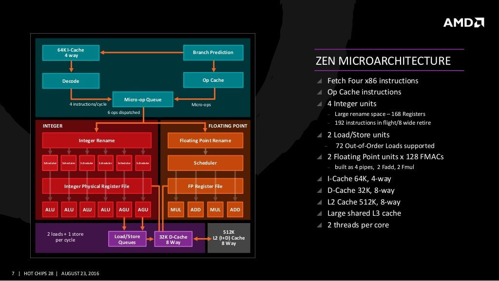
The overall instruction and data flow in the Zen core is given as follows. In the front-end we have the instruction cache, branch predictor, decode and the Operations cache. In the back-end, the data is fed into the integer and the floating point engines. In the integer engine, data is fed into six schedulers which then feed the data into the 4 ALU (arithmetic logic unit)or 2 AGU( Address Generation Unit). For floating point operations, data is fed into the Floating Point unit which then schedules the tasks and sends it to the FMUL or FADD units, of which there are 2, 128-bit wides. They can together work in unison to execute a single 256 bit floating point operation. Finally, the output is sent to the Data cache, and consequently the L2. This completes one data cycle in the Ryzen processor.

Another major change in Zen was that AMD introduced micro-op cache in its processors for the first time. I don’t think that AMD disclosed any particular size for this cache—usually it is very small. Fortunately, Anandtech did our work for us. It is a 2048 wide uOps cache (i.e. can support 2048 micro operations) with each cache line holding upto 8 operations. Intel has been using micro op cache since its Sandy Bridge cores. A uOps cache stores instructions decoded from the decoders or the I cache. When an instruction needs to be decoded, the uop cache is checked for its decoded form which is re-used if cached. If it is not available, the instruction is decoded and then cached.
Another new factor that AMD introduced with the Zen core is the new “Infinity Fabric”. It reminds me of the Nvidia NVlink that IBM uses in their power series of processors. It was detailed in April 2017 by AMD CTO Mark Papermaster. It consists of two parts—Scalable Data Fabric(SDF) and Scalable Control Fabric(SCF). SDF connects the different end points, including the Non-Uniform Memory Accesses(NUMA’s), PHY’s and any other accelerators that is compatible with Infinity Fabric. In essence, this is what HyperTransport have evolved into. The SCF transmits many system control signals – this includes things such as thermal and power management, tests, security, and 3rd party IP. AMD claims that this can efficiently scale over to 64 cores with negligible performance loss. It can also be used to connect AMD’s graphics portfolio, which includes—but is not limited to— AMD’s upcoming Vega processing units.
For intra-chip communications, AMD’s Infinity Fabric (IF) is tied to the chip’s PCIe links, and uses the Global Memory Interconnect. This allows the CPU cores to make use of the added power when workloads are not utilizing the entire fiber’s bandwidth. There is a bi-directional bandwidth of about 40GB/s (~39.74 GB/s). This is the bandwidth of dual channel DDR4 memory at 2666 MT/s. The underlying techniques (Single-ended signalling/differential SerDes) processes are highly advanced sophisticated connection techniques and are beyond the scope of this discussion.


Apart from all the technological advancements, AMD’s new Ryzen processors also use a new 14nm finfet node from Globalfoundries. It is the same 14nm LPP that Globalfoundries licensed from Samsung. This has enabled high die sizes of nearly 200mm^2 with very low power consumption. Also, AMD chose to not include any graphics engine in their initial Summit Ridge dies. This has resulted in a 8 core die with a 20mb total cache and a very high clock speed of 4 Ghz, all within a 95 watt TDP. Actual power consumption figures may vary on the setup and the overclock used. AMD has declared that the same Zen core will scale TDP ranges all the way from 4W to 95W.
Unboxing the Ryzen 1700X
Test System
Before we jump into performance numbers. Heres a look at the test system we used:
- Ryzen R7 1700X
- MSI B350 Gaming Pro Carbon
- 16GB DDR4 @2666 MHz
- Kingston SSDNow V300 240GB
- AMD RX570 4GB DDR5 GPU
- CoolerMaster V1000 PSU
Performance
We ran the CPU through the short version of our benchmark gauntlets for now. We will be adding more tests into it so don’t forget to check back in a while.
Aida 64 CPU

Here we are seeing the R7 1700X going toe to toe with the much expensive Core i7 6950X in most cases, even edging it out on some. Which shows the improvements in the IPC department as well as multicore efficiency.
CineBench R15

Here also we see similar performance. The Ryzen keeping up with its competitor and edging past it by a healthy margin.
GeekBench 4

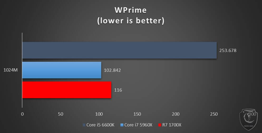
WPrime

Overall we are seeing healthy competition across the boards and with its price advantage we have no qualms declaring AMD as the winner here.
Editors Note : We will be adding a few more real word tests into the mix, so check back in a while.
Conclusion
It is clearly indicative that after a long wait of a decade, we can finally stand on this soil, and conclude that AMD IS BACK! Yes guys, you heard us right. AMD is back, and it is back with a bang! Completely disrupting the performance segments on anything remotely productive, providing strong, competitive performance to other CPUs that are far above its price class. With a very competitive architecture, AMD has finally delivered on its promise of providing a 40% uplift to its IPC, and then some more. But what is the road ahead? AMD promises us further IPC improvements in their next iteration of Zen, to be named as Zen 2. How they deliver on that performance is yet to be seen, but for now, they sure deserve a huge round of applause from everyone in the pc landscape. Gone are the days when people only used to look at the blue camp while building a multi purpose workstation PC, now we have a new contender in town!
Thank you, people, for being with us through this ride. For their disruptive and market defining performance in a genre changing price segment, we award AMD our prestigious Gold award.


