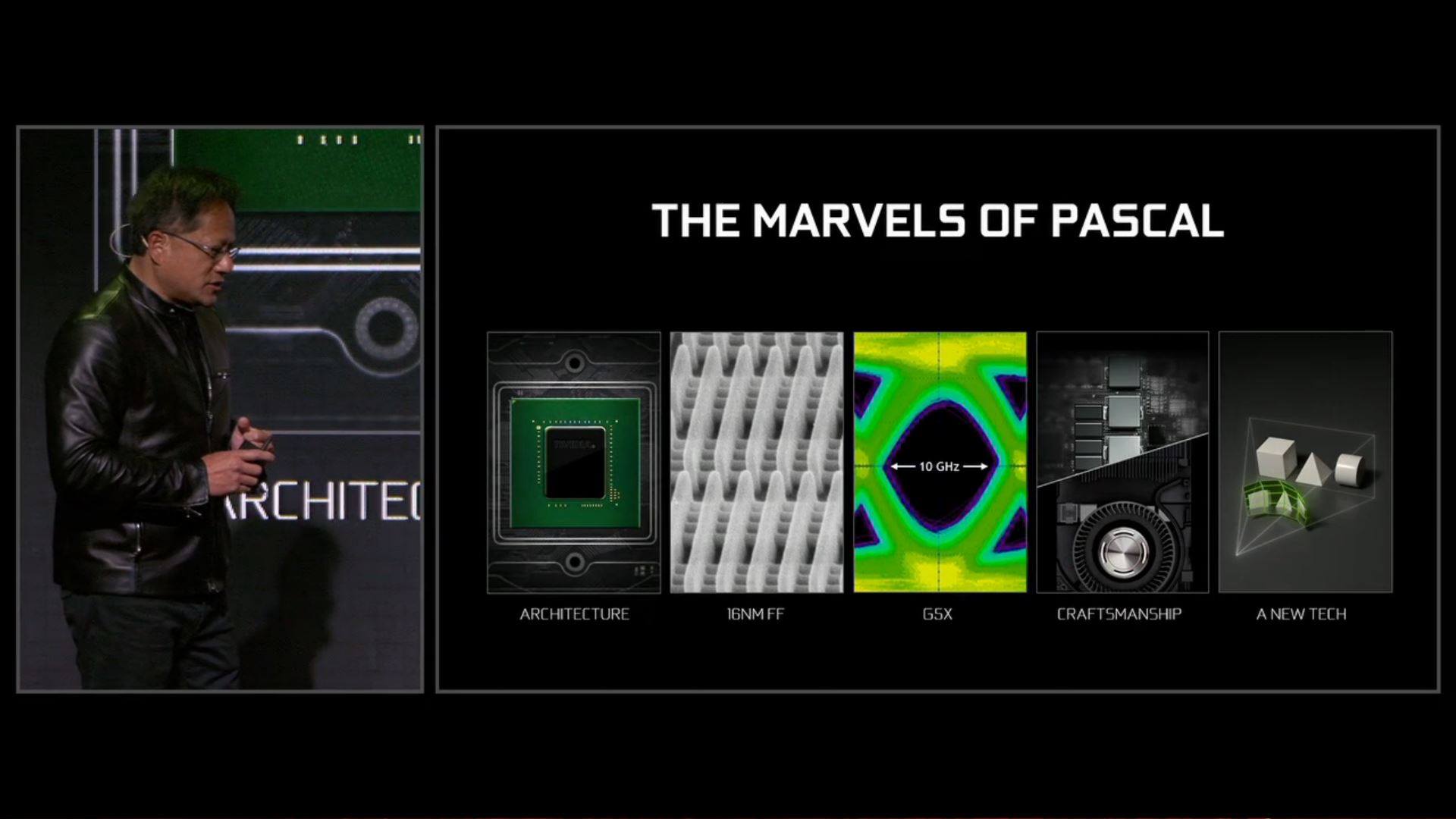
Nvidia has announced their latest graphics cards based on the Pascal architecture, the GTX 1080 and GTX 1070. Both cards are built on TSMC’s 16nm FinFEt technology and bring a wide array of revolutionary performance and efficiency improvement over the Maxwell architecture. Nvidia claims the GTX 1080 provides significantly faster performance over the Titan X with a TDP of only 180 Watts.

Nvidia is touting a “groundbreaking new design” with a new, sleek look for the 1080 cooler shroud, updated from the NVTTM design used in Kepler and Maxwell graphics cards. Nvidia promises that the new cards will be able to play 4K games with respectable frame rates and image quality compared to the Maxwell GPUs.


The GTX 1080 is powered by the GP104 GPU, successor to the GM204 which was used in the GTX 980 graphics card, but thanks to the 16nm FinFET manufacturing process, Nvidia has been able to increase transistor density significantly while improving performance at minimal power consumption hits.
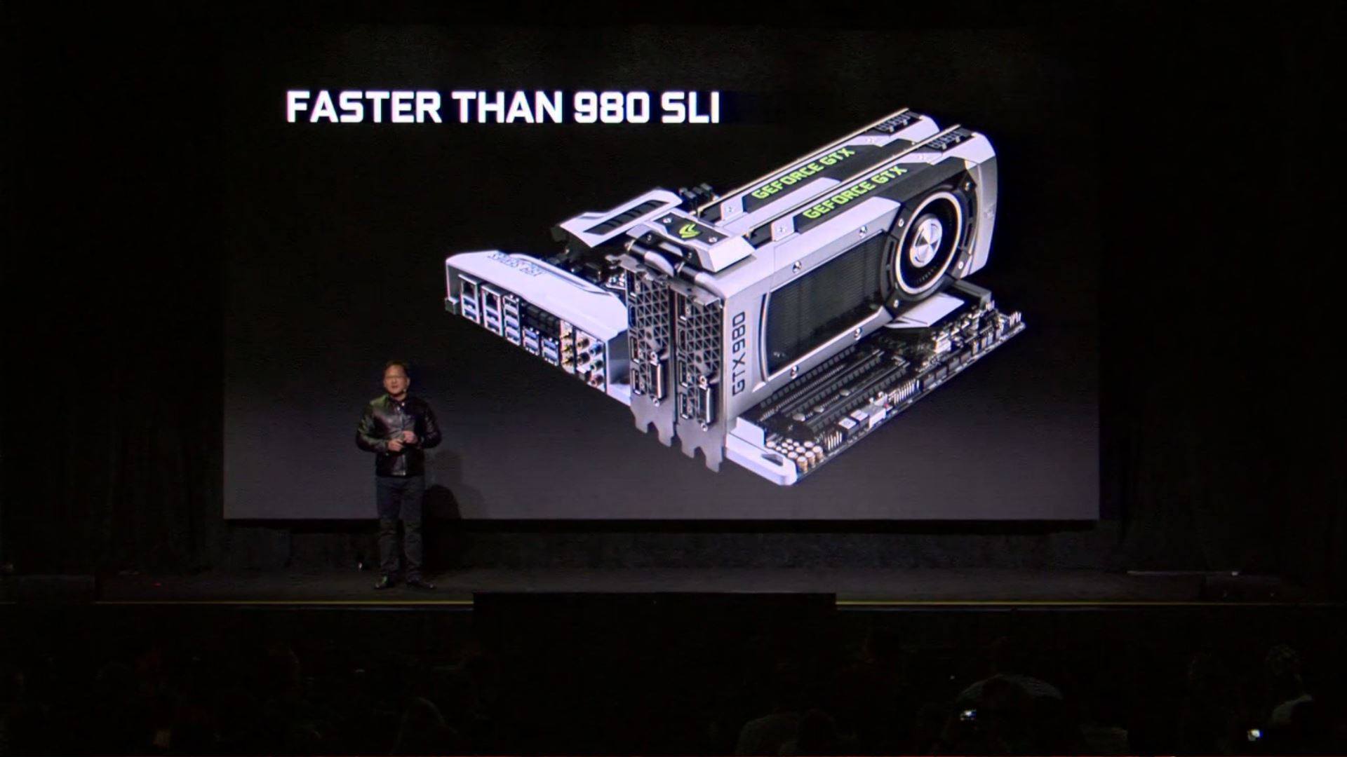
The performance of NVIDIA’s GeForce GTX 1080 is just off the charts. NVIDIA’s CEO, Jen-Hsun, mentioned at the announcement that the GeForce GTX 1080 is not only faster than one GeForce GTX 980 but it crushes two 980s in SLI, all thanks to the massive jump from the 28nm tech to 16nm.
Thanks to a mix of the new cooler and an insanely efficient process, the GTX 1080 can be overclocked to an incredible 2.1 GHz on air, while remaining under manageable temperatures, on air cooling.

But that’s just the tip of the iceberg, the performance metrics don’t stop at the 980. Compared to the GeForce GTX Titan X which is a 8 billion transistor behemoth with 3072 CUDA Cores, the NVIDIA GeForce GTX 1080 is a whole lot faster. This means we have a new champ from NVIDIA in the market that beats the GeForce GTX 980 Ti and the GeForce GTX Titan X at just 180W.

The NVIDIA GeForce GTX 1080 features the GP104 GPU (GP104-400-A1) core which comprises of 2560 CUDA cores. NVIDIA’s FinFET architecture allows significant increase in clock frequency increase. The GeForce GTX 1080 was shown clocking in at 2.1 GHz clock speeds on air cooling.
The actual clock speeds are maintained at 1607 MHz base and 1733 MHz boost but the FinFET architecture allows for extreme overclocking as demoed at the event. The chip features 8 GB of GDDR5X memory featured across a 256-bit bus and clocked at 10 GB/s. This leads to a total bandwidth of 320 GB/s.

Nvidia also showed off a new SLI bridge, called the HB-SLI, which “doubles the available bandwidth compared to the Maxwell SLI bridges” allowing for silky-smooth gaming sessions. The new bridge will be available for the GTX 1080 on release on May 27.

The full specs of the GTX 1080 are given below:
Display Support:
Maximum Digital Resolution: 7680×4320@60Hz
Maximum GPU Tempurature (in C): 94
Recommended System Power (W): 500 W