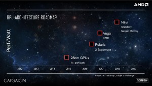
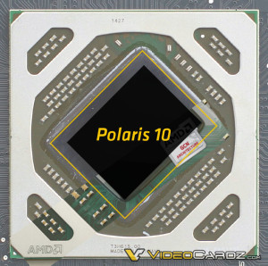
AMD (NASDAQ: AMD) has launched a new page on their website, dedicated to their forthcoming Polaris GPU architecture, with one especially interesting tidbit: a partial shot of the Polaris die. the folks over at Videocardz were able to produce a complete die shot from it, along with providing an estimation of the die size. Their estimates correspond to an earlier leak (which was quickly taken down) and presumably confirms that the Polaris 10 die will be 233 mm2 in size.
AMD has teased die shots of its upcoming GPUs in the past, Fiji being the most recent example and they were successfully analyzed to give an accurate representation of not only the die but its components as well. In what appears to be history repeating itself, AMD has published teasers of both Polaris 10 ad Polaris 11 on its new page. Given below are the die reconstructions courtesy of Videocardz:
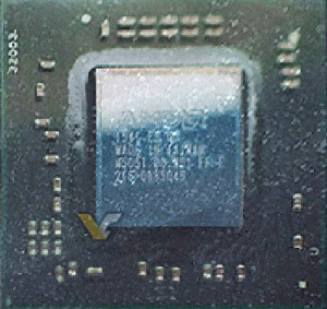
 According to AMD, Polaris 11 will be positioned at the entry level desktop and mainstream notebook segments, and the bigger Polaris 10 will be positioned at the mainstream desktop and high-end notebook segments. The expected TDP of Polaris 11 (codenamed Baffin) is at an impressive 50 Watts and the TDP of the Polaris 10 (codenamed Ellsemere) is expected between 110 and 150 Watts.
According to the information known about the 14nm LPP process, and based on transistor density increase, a 232mm² GPU would be roughly equivalent to a 464mm² 28nm processor – at the same TDP levels. Since we already know that AMD is going to be focusing not just on performance but power efficiency as well, it may well be possible that this number could be much higher.
AMD has also been significantly touting a 2.5x increase in efficiency over their previous generations. If that number is correct, then theoretically speaking, the Polaris 10 GPU should be able to provide the same performance as a 580mm2 die. However, accounting for leakage when clocking at high rates, the actual numbers may be lower than the estimates given by AMD. Also, we do not know what kind of power efficiency mix AMD is playing with here so it would be pointless to speculate further about the exact performance levels at this point, especially considering that AMD is expected to fully announce Polaris at Computex.
The Estimated specifications of the Polaris 10 and Polaris 11 based video cards are given below. Polaris 11 is expected to be used n 6 dGPUs and Polaris 10 in 2 dGPUs.
Please note that the specifications are purely speculations based on previous generation GPUs and leaks, and official specifications will only be available when AMD announces the Polaris GPUs, possibly at Computex.
| Specifications | Radeon R9 480X | Radeon R9 480 | Radeon R9 470X | Radeon R9 470 |
|---|---|---|---|---|
| GPU | Polaris 10 / Ellesmere XT | Polaris 10 / Ellesmere Pro | Polaris 11 / Baffin XT | Polaris 11 / Baffin Pro |
| Fabrication Process | 14nm FinFET | 14nm FinFET | 14nm FinFET | 14nm FinFET |
| Compute Units | 40 | 36 | 20 | 16 |
| GCN Generation | GCN 4.0 | GCN 4.0 | GCN 4.0 | GCN 4.0 |
| Stream Processors | 2560 SPs | 2304 SPs | 1280 SPs | 1024 SPs |
| Memory Bus | 256-bit | 256-bit | 128-bit | 128-bit |
| Memory | 8GB GDDR5/X | 8GB GDDR5/X | 4GB GDDR5/X | 4GB GDDR5/X |
| TDP | ~110-150W | ~110-150W | <50W | <50W |
Sources: AMD and VideoCardz


