Introduction
Since TSMC has done nothing in terms of shrinking of manufacturing process in the last 3 years, it was always a challenge for the GPU manufacturers to pack more efficient architecture within the same 28nm manufacturing process.
Nvidia showed off their first generation Maxwell part in the form of GTX 750 and GTX 750Ti where they have pulled off an unbelievable amount of performance at a very low power envelope, something which is not yet fully been answered by AMD.
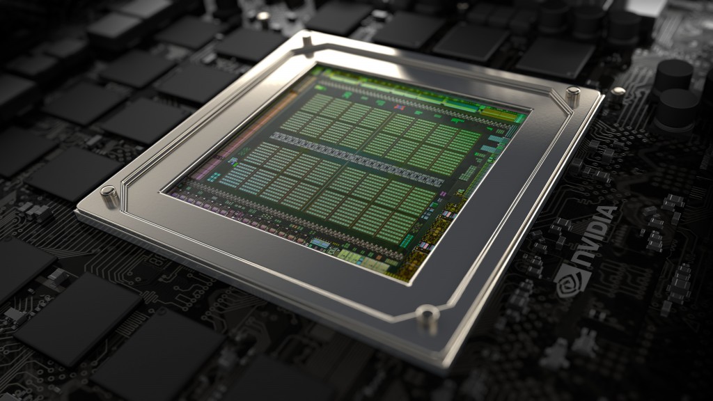
We will be reviewing the second generation Maxwell GPUs, GM204 in its gaming-oriented flagship, the GTX980.
GM 204 follows up on the earlier GM107,along with a few tweaks and tricks of its own which truly makes it Maxwell V2.We will know about it in detail but first let us take a look at what we have today and where exactly it stands in reference to the older Nvidia Cards.
| NVIDIA GPU Specification Comparison | ||||
|---|---|---|---|---|
| GTX 980 | GTX 970 (Corrected) | GTX 780 Ti | GTX 770 | |
| CUDA Cores | 2048 | 1664 | 2880 | 1536 |
| Texture Units | 128 | 104 | 240 | 128 |
| ROPs | 64 | 56 | 48 | 32 |
| Core Clock | 1126MHz | 1050MHz | 875MHz | 1046MHz |
| Boost Clock | 1216MHz | 1178MHz | 928Mhz | 1085MHz |
| Memory Clock | 7GHz GDDR5 | 7GHz GDDR5 | 7GHz GDDR5 | 7GHz GDDR5 |
| Memory Bus Width | 256-bit | 256-bit | 384-bit | 256-bit |
| VRAM | 4GB | 4GB | 3GB | 2GB |
| FP64 | 1/32 FP32 | 1/32 FP32 | 1/24 FP32 | 1/24 FP32 |
| TDP | 165W | 145W | 250W | 230W |
| GPU | GM204 | GM204 | GK110 | GK104 |
| Transistor Count | 5.2B | 5.2B | 7.1B | 3.5B |
| Manufacturing Process | TSMC 28nm | TSMC 28nm | TSMC 28nm | TSMC 28nm |
| Launch Date | 09/18/14 | 09/18/14 | 11/07/13 | 05/30/13 |
| Launch Price | $549 | $329 | $699 | $399 |
The top end GM 204 consists of of two cards as of now, the GTX 980 and its slightly cut-down sibling GTX 970 which from an NVIDIA product stand point will replace GTX 780/780Ti and GTX 770 respectively.
The top end part is GTX 980,which looks to be roughly 10% faster than the GTX 780Ti purely by specs while consuming about 1/3rd power.This puts the GTX 980 as the fastest single GPU now but at a price.
Maxwell 1 : the birth of GM107
Before we jump to GTX 980’s specifics and performance in games, let us look back into Maxwell 1 and the GM107 chip which started it all.
GM107 or as we call it the Maxwell V1 was the end product of the “mobile-first” design philosophy of Nvidia.
The mobile SOC market is practically unforgiving where one has to keep the power and thermal consideration in the forefront and then design a GPU around these considerations. This philosophy led Nvidia to design the GPU lineup bottom-up where they can design it for the mobile first and then scale it up for GeForce desktop/laptop segment.
Maxwell in itself is not very different form the erstwhile Kepler architecture. What Nvidia did was to rework the old architecture with a few new design tweaks to increase efficiency.
They went fromm this

to this
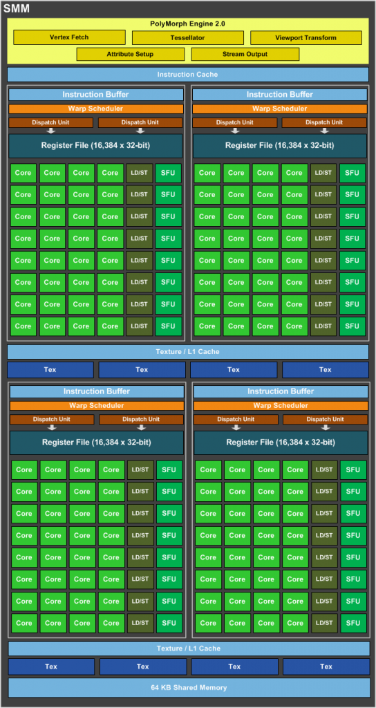
We can clearly see a couple of tweaks done in the die level.
The Kepler SMX was flat design with 4 warp schedulers and 15 different execution blocks, while the SMM has been partitioned. Physically each SMM is still one unit but logically the execution blocks accessed by warp schedulers have been marked.
The next tweak is forgoing of shared resources, while they are very good in situation when you have the workload to fill them up, they are pretty useless and feeds on unnecessary power when not being used.So while Nvidia has lost a bit of performance they make up for it in terms of power and space efficiency.
And the last but not the least, there are some tweaks made in terms of IPC by Nvidia,the scheduler has been rewritten to make it more efficient. And on the memory side of things we see in increase of L2 cache, from 256KB in GK107 to 2MB on GM107 and on GM204 it went from 512KB(GK104) to 2MB. There is also some die level optimization but Nvidia wouldn’t make that public.
Introducing GM204:
With the main Maxwell architecture taken care of lets dive into the Maxwell V2,the GM204.
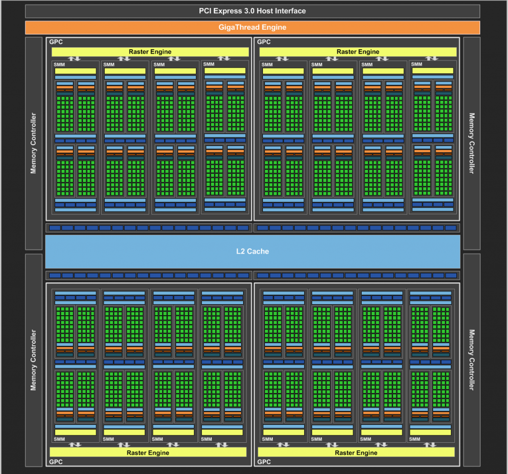
Even though a few new tricks/secret sauces were involved in the GM204, functionally its still a Maxwell GM107;just a bigger version of it with more SMM and ROP’s. This is understandable since they were working with the limitations of the ageing 28nm process and had to look for squeezing the last bits of performance from this.
While GM107 was built on 5 SMM,GM 204 is made up of 16,divided into 4GPC in place of GM 107’s one GPC. This bound to 64 ROPS’s and 4×64 bit controllers gives a 4x increase in number of ROP and 2x increase in memory bus.
In terms of design GM204 SMM is identical to the GM107 SMM, however GM204 has 96KB of shared memory while GM107 has 64KB. The polymorph engine also is updated.
Other than that the die includes use of 4 shared texture units per 2 SMMs, leading to a 16:1 ROP:MC ratio, and a 512Kb register file for each SMM.
One of the main changes form GM 107 is the increase of ROP:MC ratio in GM 204. i went form 8:1 to 16:1, last such changes were introduced when GDDR5 was introduced.
| ROP To Memory Controller Ratios | ||
|---|---|---|
| GPU | ROP:MC Ratio | Total ROPs |
| Maxwell (GM204) | 16:1 | 64 |
| Maxwell (GM107) | 8:1 | 16 |
| Kepler (GK110) | 8:1 | 48 |
| Fermi (GF110) | 8:1 | 48 |
| GT200 | 4:1 | 32 |
With that aside let’s take a look at the card itself.
GTX 980 Showcase
I will let the pictures do the talking since there is not much to say about the card. The design philosophy follows the same ones we have been accustomed to with the GTX Titan/780/770/780Ti days though NVidia for some reason has stopped using vapour chamber based cooling.
Here you can see the GTX 980 in its natural habitat,roaming freely…unbound….o wait..wrong show!
Nvidia retains the single fan design from its earlier version with the blower slightly offset to the right to suck in air, pass it over the chip and VRAMs and finally pushing it out through the brackets.
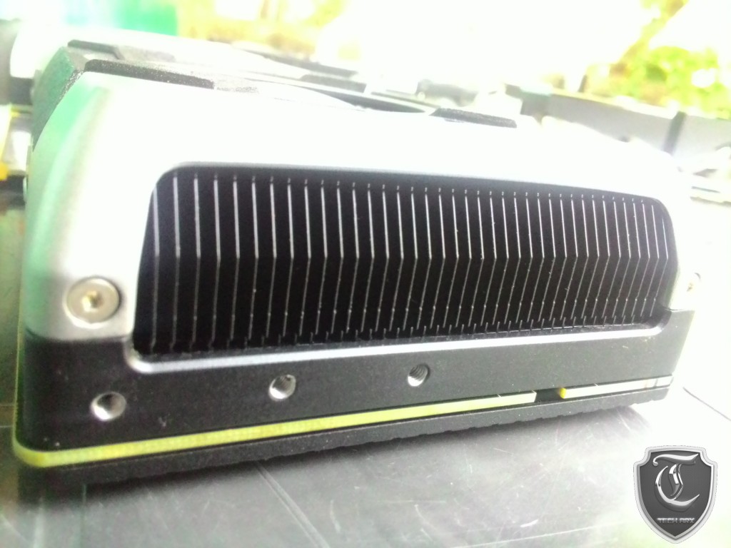 The intake looks like one half of the BMW grills to me.
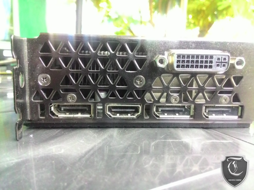
On the output part of things we see quite a nice assortment, 1x DVI-D, 1x HDMI 2.0 and 3x DisplayPort 1.2 ports.
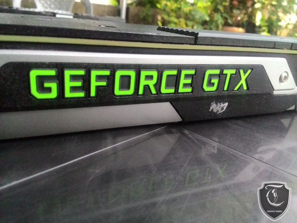
Not much to say about the logo,except the fact that you can control the LED through Nvidia GeForce Experience, where you can make it glow steadily or along with the beat of sound playing in your system.
Gaming Performance
First a little about overlcocking, even though we could overclock the card by a few MHz, overclocking the referencing is not all easy since you have a locked bios;also the reference cooler doesn’t really give much lenience to overclocking.
You can fry a few marsh mellows on the exhaust..albeit pretty slowly.
This is where we stopped in our overclocking adventure.
http://www.techpowerup.com/gpuz/details.php?id=c3f8r
The end overclock was 13% on Core and 6% on memory.
Bioshock Infinite
Ultra Settings
Ultra + DDOF

Hitman Absolution
Ultra Settings
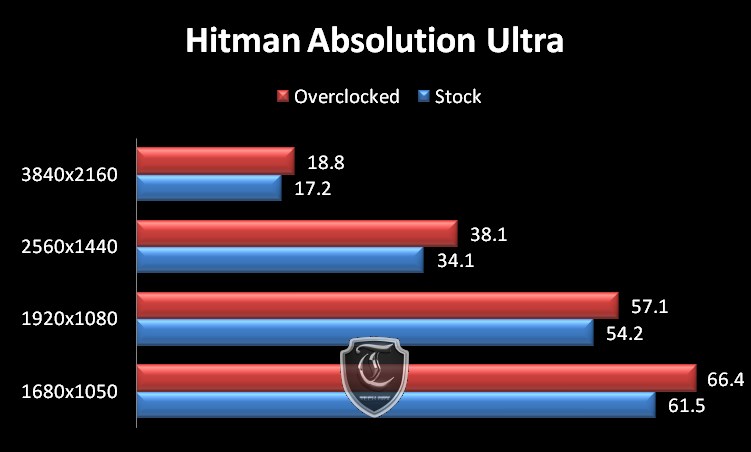
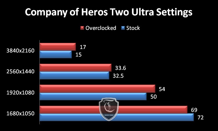
Company Of Heroes 2
Ultra Settings
Middle Earth : Shadow of Mordor
Ultra Settings
Metro 2033
Ultra Settings
Final words
The GTX 980 is an engineering marvel as any flagship GPU should be. Nvidia have shown that even with a 2 year old manufacturing node you can work on get extra efficiency out of it.
For the power conscious guys it’s a treat – a very good example of proper RnD and execution of design.
However at the end of the day other than the exceptional power to performance ratio, there is not much brought into the table, but then again you cannot blame a GPU vendor solely for this since at the end of the TSMC is the one who cannot grow out of the 28nm rut.
The price is eye-watering as well. For most 980s retailing northwards of 45K+ INR, this is a significant investment. I feel that NVidia somehow missed the killing blow here – if they would have priced it more aggressively, AMD’s current generation flagships would have a really hard time. At present, AMD can lower the prices and still offer value and bide time before they bring out their next gen cards.
Apart form that I cannot find any flaws in the card unless I resort to some nitpicking. The GTX980 is the fastest single GPU gaming card on the planet (notwithstanding the Titan X), and like all flagships it demands a flagship price. If that’s not your cup of tea, then this probably isn’t the card you’re looking for.
TechARX rating : 8.5/10

