AMD has stirred in a lot of discussion and clamor with the official announcement and performance reveal of their latest and greatest CPU architecture i.e. Zen. The most flatulent claims that have been made so far include 6900k level performance at similar clock speeds which AMD demonstrated with a Blender test at a side event, this Wednesday. All of this sounds alluring enough for any computer hardware enthusiast out there, but how exactly has AMD achieved such escalated levels of performance? It is fairly certain that there must be some curious wobble heads who are intrigued by this new mouth watering architecture from AMD. So, without further ado, let’s jump into the intrinsics of Zen and how it attains its stellar throughput and efficiency.
A look into the Zen Block Diagram

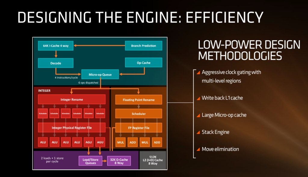
It is quite evident from the block diagram that AMD has made some humongous modifications which distinguish the upcoming Zen architecture from Bulldozer of which, the inclusion of a micro-op cache is the vital one. Other changes include the presence of a significantly larger instruction dispatcher, other caches and some vague details about the decoder.
AMD seems to have emphasized on instruction level parallelism (ILP) to a great extent this time round as the efforts on improving branch prediction appear quite patent with the slides that AMD has given away. To put it in layman’s terms, branch prediction is a technique used on modern x86 CPUs where a jump or conditional (if-else-if structure) operation’s path is predicted and executed to prevent pipeline stalls or data dependency conflicts. Bear in mind that the latter stage of the process is known as speculative execution and is not governed by the branch predictor itself. The presence of a notably efficient and larger instruction dispatcher also serves as a clear indicator of the labor that AMD has put into ameliorating single threaded performance by aiding ILP . We’ll discuss the role that the dispatcher is going to play later in this same article. For now, let’s peep into other alterations that AMD has made.
Another notable addition to the architecture is the presence of a micro-op cache which spares the instruction scheduler a ton of legwork in requesting the micro-ops that are to be implemented frequently in typical scenarios. No details have yet been entailed by AMD on the extent of the buffer of the cache but nonetheless it’s a hopeful addition considering that Intel has been successfully integrating it on their products for several generations. Earlier, inside the AMD Bulldozer architecture, the instruction scheduler would have to request the micro-ops from other neighboring caches which induced additional latency. The implementation of the micro-op cache on the Zen architecture is quite disparate from Intel’s however, as there will exist, individual schedulers for the Integer and FP unit unlike Intel which had a combined scheduler for the Integer and FP unit.
Now, to chime in on the instruction scalability that Zen offers, it’s noteworthy that the micro-op cache would sprinkle in its own set of benefits when it comes to instruction level parallelism. AMD hasn’t unveiled a lot about the anatomy of the decoder that will be present on the Zen CPUs, but has made clear that they’ll be capable of decoding 4 instructions per cycle to feed into the operations queue. The operations queue will then pour two additional micro-ops into the micro-op cache (Quite a cryptic reason behind the overhauled throughput) equating to 6 operations / instruction cycle. This is where the newer and efficient instruction dispatcher comes in since the increased scalability demands better intuition of what instructions can be executed in parallel without stalling the pipeline.
Apart from this, the Integer side of the core execution unit will assist the ALU and the AGU – Load/Store operations. 2x 16 bit load ops while 1x 16 bit store ops can be executed per instruction cycle by the load / store units aided by the 32 KB write back L1 data cache. AMD has made a switch to write back data cache as opposed to the write through cache present on Bulldozer CPUs which was the laughingstock of all pipeline stalls. This owes to the fact that on a write through data cache, the control unit prioritizes writing back to the system memory through the L1 cache rather than routing for the execution of the next instruction in queue. The situation is reversed on a Write back data cache as the CPU waits for an opportune moment to write back to the system memory in a way that no additional overhead is induced. AMD is also boasting of an increased bandwidth on the load / store units but the magnitude of the improvement hasn’t been affirmed yet.
On the floating point side of things, the units are equipped with two MULTIPLY and two ADD ports allowing for two linked FMAC operations or a 256-bit AVX per clock cycle. AMD also plans to implement a 1.75x larger instruction scheduler for instruction fetches and 50% wider issue width for maximizing potential throughput. The wider core design to bump single threaded efficiency should also do wonders in laying out the canvas for AMD’s simultaneous multithreading implementation.
What’s the Cache?
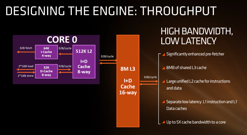
The cache blueprint is laid out in a way that the new hierarchy will only bring tremendous profits. The L3 cache is spread out among a crusade of 2 sets of 4 cores each, where each set is equipped with 8 MB / 8 Way cache summing up to a total of 16 MB L3 cache for the entire chip and 2 MB per core, exactly identical to Intel Skylake. The L2 cache is a 512 KB / 8-Way one as opposed to the 256 KB / 4-Way and 8-Way on Intel’s Skylake and Broadwell-E architecture respectively. The L1 data (L1-D) cache is a revolutionary step forward for AMD as the swap from a measly 16 KB 4-Way cache to a 32 KB 8-Way cache should help ameliorate the lower level cache performance by manifolds. The route that AMD has opted for this time round however, is the inclusion of a Write Back cache axing the previous Write through cache, something which we have detailed earlier. The L1 instruction (L1-I) cache on the other hand utilizes a 64 KB / 4-Way design and is also exclusive to each core rather than sharing resources between two cores. This culls any sort of cache miss possibilities.
Power Efficiency and Clock Gating
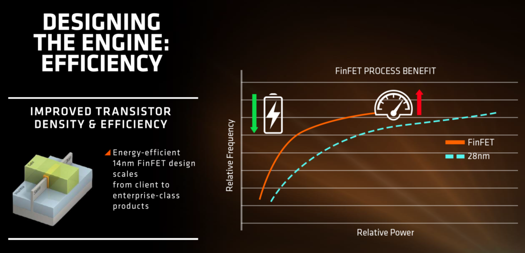
The incredible and almost implausible power efficiency escalations aren’t unknown to anyone, all of which owes to the glory of the 14nm FinFet manufacturing process – something that has already been put to the racing track with the Polaris GPUs. The switch to a smaller node size enables similar performance at phenomenally lower power consumption or gigantic performance increments at similar power consumption. Either of which will be welcomed by tech enthusiasts voluntarily. Clock gating is another technique that AMD is going to implement on the Zen CPUs to improve power efficiency. To understand what clock gating is, let us conceptualize a synchronous assembly line analogous the a synchronously clocked CPU. While the last batch for the day is prepared on the assembly line nearing its completion, even the initial stages of the line remain powered regardless of whether they are contributing to the manufacturing or not. Clock gating shuts down the dormant stages of the CPU pipeline and furnishes power only to those components which are being utilized at the particular moment. Note that the components stop drawing power only in theory as power gating presents architectural complexities that are strenuous to be eradicated.
Simultaneous Multithreading Explained
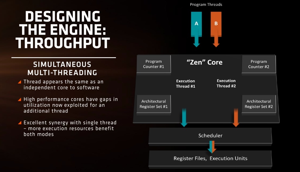
Each execution unit on a Zen CPU will support Simultaneous multithreading which allows for independent resources for the two threads that will be assigned to a core. Intel has been making exceptional use of the technology over the past few years and have named it Hyper-Threading, however, at their core, they are fundamentally indistinguishable. The implementation of Simultaneous Multithreading lists a hefty criterion, the chief prerequisite being the availability of surplus resources for each thread to operate without disrupting the other thread in pipeline. Thankfully, Zen fulfills all the demands and paves its way forward to an efficacious implementation for the tech that will be replacing CMT (Clustered Multithreading).
Source : Anandtech, Wikipedia